04.11.2024
relyon plasma @ electronica 2024
From 12 to 15 November 2024, relyon plasma will be presenting plasma technology at the stand of its parent company TDK at electronica.

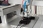
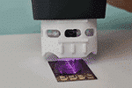
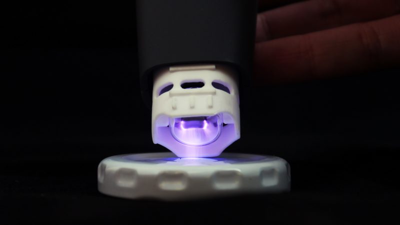
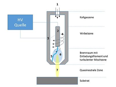
Whether for bonding or marking of plastic components, wire bonding processes on metallic contact pads or the production of energy storage devices: Adhesion plays a decisive role for product quality and process stability in many areas of the electronics industry. Plasma is increasingly being used in the electronics industry to optimally prepare the surfaces of a wide variety of materials for such adhesion processes. This technology enables selective treatment of functional surfaces on plastics, metals or composites to improve a number of subsequent processes. While conventional atmospheric pressure plasma systems must be permanently integrated into systems with appropriate gas supply, extraction and safety concepts, the cold plasma handheld device piezobrush® PZ3 offers the possibility of uncomplicated and manual optimization of surfaces.
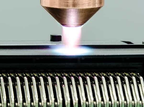
Plasma activation of sensitive electronics is possible with the high-performance plasma system plasmabrush® PB3. The low-potential A250 was specially developed for use on electronic components for activation or cleaning.
The surface energy of individual components and assemblies varies greatly. Plasma treatment can increase the total surface energy, resulting in more homogeneous wetting. So we can proudly say: plasma activation and electronics are possible!
Key Word Search