Plasma activation and electronic components – it works!
Whether the mobile or in the washing machine – everywhere you now find PCBs. It all seems to have been invented, but developers and manufacturers are faced with even smaller and more extensively populated boards.
For this purpose, most carrier materials are made of glass fiber reinforced plastic which often has a low surface energy (about 40-45 mN / m). This can be with teflon based PCB or polyester films even lower. A plasma treatment improves this surface energies up to 72 mN / m. Thus, subsequent bonding processes or the application of conformal coatings are supported.
Treatment of assembled printed circuit boards
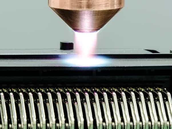
The encapsulation of assembled printed circuit boards usually proves to be difficult. The surface energy of individual components and assemblies varies greatly. Plasma treatment can increase the total surface energy, resulting in a more homogeneous wetting. The adhesion is to be improved by plasma treatment and the associated higher wetting. The PB3 system with nozzle A250 and nitrogen as process gas is investigated in this case. A measure of the improvement can be demonstrated by reducing the contact angle. A Krüss Drop Shape Analyser DSA 10 is used for analysis.
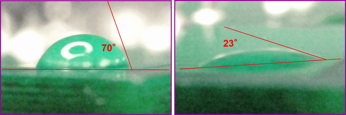
Plasma treatment for a good hydrophilization of the surface. The contact angle is reduced from 70° to 23°. Sometimes the height of the components can be greater than 30mm. The working distance between PCB and nozzle is therefore >50mm.
My board is however already fitted! – Plasma activation and electronic?
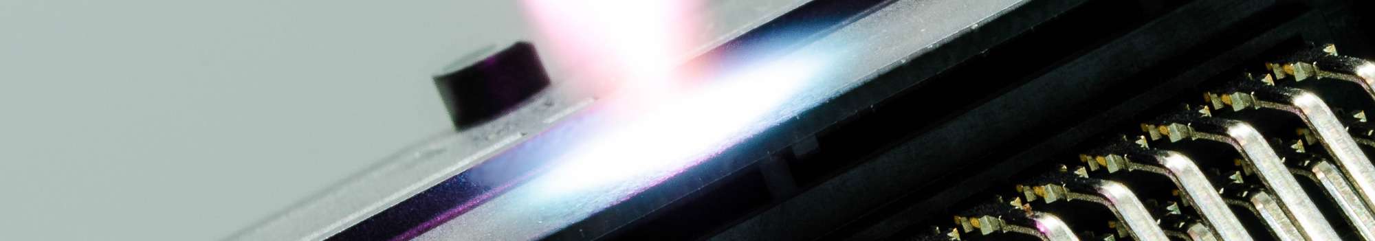
Plasma activation and electronics are no longer a problem with our A250 nozzle model. This model has been optimized for use on electronic components for activation or cleaning. This nozzle for sensitive materials is used with the plasmabrush® PB3 System and PAA® technology. The encapsulation of assembled printed circuit boards usually proves to be difficult. The surface energy of individual components and assemblies varies greatly. Plasma treatment can increase the total surface energy so that more homogeneous wetting is possible. So we can proudly say: plasma activation and electronics it works!