04.11.2024
relyon plasma @ electronica 2024
From 12 to 15 November 2024, relyon plasma will be presenting plasma technology at the stand of its parent company TDK at electronica.

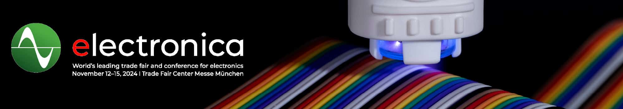
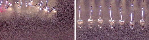
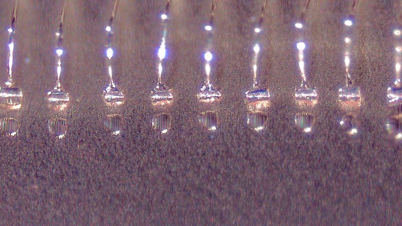
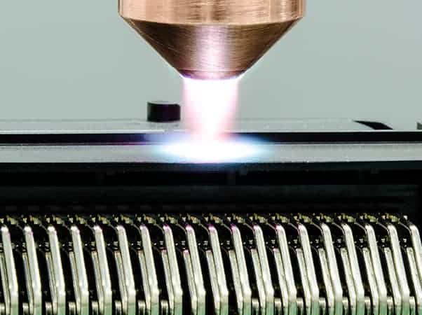
Semiconductor technology and plasma? Cold atmospheric pressure plasma is used in many semiconductor manufacturing processes. A semiconductor is a solid material with electric properties in between those of conductors and insulators. The goal of plasma treatment is the finecleaning of semiconductor components and plasma activation, which leads to an increase in surface energy.
Key Word Search